Collection
Technology Trends
2026.09.07
Names of Semiconductor Equipment You Should Know Before Nanometers
Eight Types of Actual Manufacturing Equipment that Draw, Etch, Stack, and Inspect with Light
The semiconductor process is not about a single machine completing a wafer. Hundreds of steps connect the lithography that draws circuits, etching that removes unnecessary parts, deposition that layers films, and testing equipment that detects defects and verifies completed chips. This list connects the names and roles of actual commercial equipment that represents each process.
The focus is on understanding the flow of processes rather than price rankings. It includes ASML's EUV equipment, process equipment from Applied Materials, Lam Research, and Tokyo Electron, KLA's inspection systems, Hanmi Semiconductor's HBM packaging equipment, and Advantest's testing platforms. Specifications are based on the manufacturer's official pages, and specific deployment information from customer companies is not estimated.
The focus is on understanding the flow of processes rather than price rankings. It includes ASML's EUV equipment, process equipment from Applied Materials, Lam Research, and Tokyo Electron, KLA's inspection systems, Hanmi Semiconductor's HBM packaging equipment, and Advantest's testing platforms. Specifications are based on the manufacturer's official pages, and specific deployment information from customer companies is not estimated.
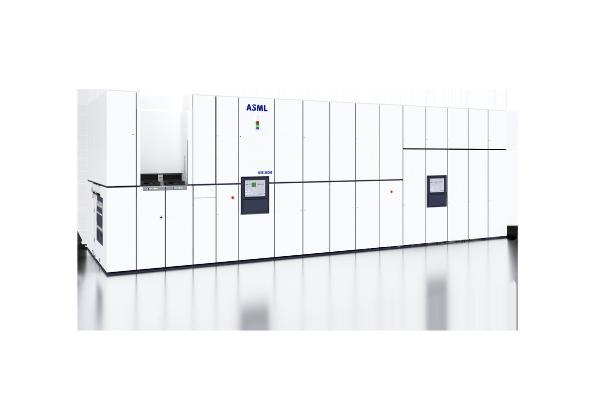
ASML TWINSCAN NXE:3800E
The ASML TWINSCAN NXE:3800E is an item to consider in 'Names of Semiconductor Equipment You Should Know Before Nanometers.' A lithography product. It is a lithography system that supports the mass production of 2nm logic and cutting-edge DRAM using a 13.5nm EUV light source. It increases productivity and overlay precision at the stage of transferring circuit patterns onto wafers. This list reads the actual role of ASML TWINSCAN NXE:3800E from the perspective of 'eight types of actual manufacturing equipment that draw, etch, stack, and inspect with light.' Even when comparing similar items, it's crucial to first distinguish the purpose and state of ASML TWINSCAN NXE:3800E.
The item information of ASML TWINSCAN NXE:3800E is classified as type: Lithography · Main purpose: 0.33 NA EUV · Checkpoint: Mass production. Each value of ASML TWINSCAN NXE:3800E answers different questions, so it shouldn't be lined up with other products just by generational name or a single high-performance phrase. Distinction must be made regarding whether ASML TWINSCAN NXE:3800E is at the announcement, sample, mass production, or actual application stage, and performance values must be viewed along with conditions such as precision, power, and configuration.
Let’s first note what data movement or process bottlenecks ASML TWINSCAN NXE:3800E reduces. Then, comparing ASML TWINSCAN NXE:3800E with other items in this list based on application environment, power, software, or manufacturing stages will clarify its distinct role. The manufacturer’s description of ASML TWINSCAN NXE:3800E is only the starting point for confirming functions and does not guarantee perceived performance. Reading ASML TWINSCAN NXE:3800E in this order allows us to explain both the reasons for its attention and its limitations.
The item information of ASML TWINSCAN NXE:3800E is classified as type: Lithography · Main purpose: 0.33 NA EUV · Checkpoint: Mass production. Each value of ASML TWINSCAN NXE:3800E answers different questions, so it shouldn't be lined up with other products just by generational name or a single high-performance phrase. Distinction must be made regarding whether ASML TWINSCAN NXE:3800E is at the announcement, sample, mass production, or actual application stage, and performance values must be viewed along with conditions such as precision, power, and configuration.
Let’s first note what data movement or process bottlenecks ASML TWINSCAN NXE:3800E reduces. Then, comparing ASML TWINSCAN NXE:3800E with other items in this list based on application environment, power, software, or manufacturing stages will clarify its distinct role. The manufacturer’s description of ASML TWINSCAN NXE:3800E is only the starting point for confirming functions and does not guarantee perceived performance. Reading ASML TWINSCAN NXE:3800E in this order allows us to explain both the reasons for its attention and its limitations.
종류 노광
주요 용도 0.33 NA EUV
확인 포인트 양산
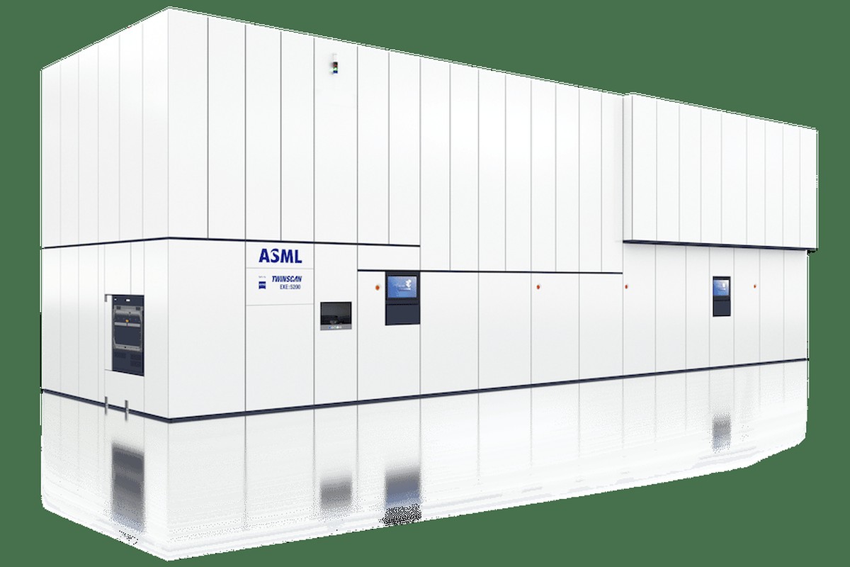
ASML TWINSCAN EXE:5200B
The ASML TWINSCAN EXE:5200B is an item to consider in 'Names of Semiconductor Equipment You Should Know Before Nanometers.' A lithography product. This next-generation lithography system uses 0.55 NA High-NA EUV and serves as a key to securing mass production throughput while implementing smaller patterns. This list reads the actual role of ASML TWINSCAN EXE:5200B from the perspective of 'eight types of actual manufacturing equipment that draw, etch, stack, and inspect with light.' Even when comparing similar items, it's crucial to first distinguish the purpose and state of ASML TWINSCAN EXE:5200B.
The item information of ASML TWINSCAN EXE:5200B is classified as type: Lithography · Main purpose: High-NA EUV · Checkpoint: Mass production. Each value of ASML TWINSCAN EXE:5200B answers different questions, so it shouldn't be lined up with other products just by generational name or a single high-performance phrase. Distinction must be made regarding whether ASML TWINSCAN EXE:5200B is at the announcement, sample, mass production, or actual application stage, and performance values must be viewed along with conditions such as precision, power, and configuration.
Let’s first note what data movement or process bottlenecks ASML TWINSCAN EXE:5200B reduces. Then, comparing ASML TWINSCAN EXE:5200B with other items based on application environment, power, software, or manufacturing stages will clarify its distinct role. The manufacturer’s description of ASML TWINSCAN EXE:5200B is only the starting point for confirming functions and does not guarantee perceived performance. Reading ASML TWINSCAN EXE:5200B in this order allows us to explain both the reasons for its attention and its limitations.
The item information of ASML TWINSCAN EXE:5200B is classified as type: Lithography · Main purpose: High-NA EUV · Checkpoint: Mass production. Each value of ASML TWINSCAN EXE:5200B answers different questions, so it shouldn't be lined up with other products just by generational name or a single high-performance phrase. Distinction must be made regarding whether ASML TWINSCAN EXE:5200B is at the announcement, sample, mass production, or actual application stage, and performance values must be viewed along with conditions such as precision, power, and configuration.
Let’s first note what data movement or process bottlenecks ASML TWINSCAN EXE:5200B reduces. Then, comparing ASML TWINSCAN EXE:5200B with other items based on application environment, power, software, or manufacturing stages will clarify its distinct role. The manufacturer’s description of ASML TWINSCAN EXE:5200B is only the starting point for confirming functions and does not guarantee perceived performance. Reading ASML TWINSCAN EXE:5200B in this order allows us to explain both the reasons for its attention and its limitations.
종류 노광
주요 용도 High-NA EUV
확인 포인트 양산 도입
Applied Materials Centura Sculpta
The Applied Materials Centura Sculpta is an item to consider in 'Names of Semiconductor Equipment You Should Know Before Nanometers.' A patterning product. It is a patterning equipment that selectively alters pattern forms to complement some EUV double patterning. It shows an approach to reducing lithography counts and process complexity. This list reads the actual role of Applied Materials Centura Sculpta from the perspective of 'eight types of actual manufacturing equipment that draw, etch, stack, and inspect with light.' Even when comparing similar items, it's crucial to first distinguish the purpose and state of Applied Materials Centura Sculpta.
The item information of Applied Materials Centura Sculpta is classified as type: Patterning · Main purpose: Pattern shaping · Checkpoint: Mass production equipment. Each value of Applied Materials Centura Sculpta answers different questions, so it shouldn't be lined up with other products just by generational name or a single high-performance phrase. Distinction must be made regarding whether Applied Materials Centura Sculpta is at the announcement, sample, mass production, or actual application stage, and performance values must be viewed along with conditions such as precision, power, and configuration.
Let’s first note what data movement or process bottlenecks Applied Materials Centura Sculpta reduces. Then, comparing Applied Materials Centura Sculpta with other items based on application environment, power, software, or manufacturing stages will clarify its distinct role. The manufacturer’s description of Applied Materials Centura Sculpta is only the starting point for confirming functions and does not guarantee perceived performance. Reading Applied Materials Centura Sculpta in this order allows us to explain both the reasons for its attention and its limitations.
The item information of Applied Materials Centura Sculpta is classified as type: Patterning · Main purpose: Pattern shaping · Checkpoint: Mass production equipment. Each value of Applied Materials Centura Sculpta answers different questions, so it shouldn't be lined up with other products just by generational name or a single high-performance phrase. Distinction must be made regarding whether Applied Materials Centura Sculpta is at the announcement, sample, mass production, or actual application stage, and performance values must be viewed along with conditions such as precision, power, and configuration.
Let’s first note what data movement or process bottlenecks Applied Materials Centura Sculpta reduces. Then, comparing Applied Materials Centura Sculpta with other items based on application environment, power, software, or manufacturing stages will clarify its distinct role. The manufacturer’s description of Applied Materials Centura Sculpta is only the starting point for confirming functions and does not guarantee perceived performance. Reading Applied Materials Centura Sculpta in this order allows us to explain both the reasons for its attention and its limitations.
종류 패터닝
주요 용도 Pattern shaping
확인 포인트 양산 장비

Lam Research Akara
The Lam Research Akara is an item to consider in 'Names of Semiconductor Equipment You Should Know Before Nanometers.' An etching product. It is a plasma etching platform for fine logic and memory structures. It serves to precisely remove only the desired material while maintaining the shapes of deep and narrow structures. This list reads the actual role of Lam Research Akara from the perspective of 'eight types of actual manufacturing equipment that draw, etch, stack, and inspect with light.' Even when comparing similar items, it's crucial to first distinguish the purpose and state of Lam Research Akara.
The item information of Lam Research Akara is classified as type: Etching · Main purpose: Plasma etch · Checkpoint: Mass production equipment. Each value of Lam Research Akara answers different questions, so it shouldn't be lined up with other products just by generational name or a single high-performance phrase. Distinction must be made regarding whether Lam Research Akara is at the announcement, sample, mass production, or actual application stage, and performance values must be viewed along with conditions such as precision, power, and configuration.
Let’s first note what data movement or process bottlenecks Lam Research Akara reduces. Then, comparing Lam Research Akara with other items based on application environment, power, software, or manufacturing stages will clarify its distinct role. The manufacturer’s description of Lam Research Akara is only the starting point for confirming functions and does not guarantee perceived performance. Reading Lam Research Akara in this order allows us to explain both the reasons for its attention and its limitations.
The item information of Lam Research Akara is classified as type: Etching · Main purpose: Plasma etch · Checkpoint: Mass production equipment. Each value of Lam Research Akara answers different questions, so it shouldn't be lined up with other products just by generational name or a single high-performance phrase. Distinction must be made regarding whether Lam Research Akara is at the announcement, sample, mass production, or actual application stage, and performance values must be viewed along with conditions such as precision, power, and configuration.
Let’s first note what data movement or process bottlenecks Lam Research Akara reduces. Then, comparing Lam Research Akara with other items based on application environment, power, software, or manufacturing stages will clarify its distinct role. The manufacturer’s description of Lam Research Akara is only the starting point for confirming functions and does not guarantee perceived performance. Reading Lam Research Akara in this order allows us to explain both the reasons for its attention and its limitations.
종류 식각
주요 용도 Plasma etch
확인 포인트 양산 장비
Tokyo Electron Acrevia
The Tokyo Electron Acrevia is an item to consider in 'Names of Semiconductor Equipment You Should Know Before Nanometers.' An etching product. It is an etching system for 3D integration that utilizes both sides of the wafer. It targets processes needed for new chip structures, such as backside power supply and high aspect ratio structures. This list reads the actual role of Tokyo Electron Acrevia from the perspective of 'eight types of actual manufacturing equipment that draw, etch, stack, and inspect with light.' Even when comparing similar items, it's crucial to first distinguish the purpose and state of Tokyo Electron Acrevia.
The item information of Tokyo Electron Acrevia is classified as type: Etching · Main purpose: Wafer backside · Checkpoint: Product announcement. Each value of Tokyo Electron Acrevia answers different questions, so it shouldn't be lined up with other products just by generational name or a single high-performance phrase. Distinction must be made regarding whether Tokyo Electron Acrevia is at the announcement, sample, mass production, or actual application stage, and performance values must be viewed along with conditions such as precision, power, and configuration.
Let’s first note what data movement or process bottlenecks Tokyo Electron Acrevia reduces. Then, comparing Tokyo Electron Acrevia with other items based on application environment, power, software, or manufacturing stages will clarify its distinct role. The manufacturer’s description of Tokyo Electron Acrevia is only the starting point for confirming functions and does not guarantee perceived performance. Reading Tokyo Electron Acrevia in this order allows us to explain both the reasons for its attention and its limitations.
The item information of Tokyo Electron Acrevia is classified as type: Etching · Main purpose: Wafer backside · Checkpoint: Product announcement. Each value of Tokyo Electron Acrevia answers different questions, so it shouldn't be lined up with other products just by generational name or a single high-performance phrase. Distinction must be made regarding whether Tokyo Electron Acrevia is at the announcement, sample, mass production, or actual application stage, and performance values must be viewed along with conditions such as precision, power, and configuration.
Let’s first note what data movement or process bottlenecks Tokyo Electron Acrevia reduces. Then, comparing Tokyo Electron Acrevia with other items based on application environment, power, software, or manufacturing stages will clarify its distinct role. The manufacturer’s description of Tokyo Electron Acrevia is only the starting point for confirming functions and does not guarantee perceived performance. Reading Tokyo Electron Acrevia in this order allows us to explain both the reasons for its attention and its limitations.
종류 식각
주요 용도 Wafer backside
확인 포인트 제품 발표
KLA 39xx Wafer Inspection System
The KLA 39xx Wafer Inspection System is an item to consider in 'Names of Semiconductor Equipment You Should Know Before Nanometers.' An inspection product. It is an inspection platform that finds microscopic defects in patterned wafers and narrows down the causes of yield issues. The faster defects are detected, the more costs can be reduced from repeating defective processes. This list reads the actual role of KLA 39xx Wafer Inspection System from the perspective of 'eight types of actual manufacturing equipment that draw, etch, stack, and inspect with light.' Even when comparing similar items, it's crucial to first distinguish the purpose and state of KLA 39xx Wafer Inspection System.
The item information of KLA 39xx Wafer Inspection System is classified as type: Inspection · Main purpose: Patterned wafer · Checkpoint: Mass production inspection. Each value of KLA 39xx Wafer Inspection System answers different questions, so it shouldn't be lined up with other products just by generational name or a single high-performance phrase. Distinction must be made regarding whether KLA 39xx Wafer Inspection System is at the announcement, sample, mass production, or actual application stage, and performance values must be viewed along with conditions such as precision, power, and configuration.
Let’s first note what data movement or process bottlenecks KLA 39xx Wafer Inspection System reduces. Then, comparing KLA 39xx Wafer Inspection System with other items based on application environment, power, software, or manufacturing stages will clarify its distinct role. The manufacturer’s description of KLA 39xx Wafer Inspection System is only the starting point for confirming functions and does not guarantee perceived performance. Reading KLA 39xx Wafer Inspection System in this order allows us to explain both the reasons for its attention and its limitations.
The item information of KLA 39xx Wafer Inspection System is classified as type: Inspection · Main purpose: Patterned wafer · Checkpoint: Mass production inspection. Each value of KLA 39xx Wafer Inspection System answers different questions, so it shouldn't be lined up with other products just by generational name or a single high-performance phrase. Distinction must be made regarding whether KLA 39xx Wafer Inspection System is at the announcement, sample, mass production, or actual application stage, and performance values must be viewed along with conditions such as precision, power, and configuration.
Let’s first note what data movement or process bottlenecks KLA 39xx Wafer Inspection System reduces. Then, comparing KLA 39xx Wafer Inspection System with other items based on application environment, power, software, or manufacturing stages will clarify its distinct role. The manufacturer’s description of KLA 39xx Wafer Inspection System is only the starting point for confirming functions and does not guarantee perceived performance. Reading KLA 39xx Wafer Inspection System in this order allows us to explain both the reasons for its attention and its limitations.
종류 검사
주요 용도 Patterned wafer
확인 포인트 양산 검사
Hanmi Semiconductor TC BONDER Griffin
The Hanmi Semiconductor TC BONDER Griffin is an item to consider in 'Names of Semiconductor Equipment You Should Know Before Nanometers.' A packaging product. It is a device that precisely bonds thin memory dies with heat and pressure during HBM manufacturing. It illustrates why stacked packaging equipment is crucial for AI memory supply, not just in DRAM front-end processes. This list reads the actual role of Hanmi Semiconductor TC BONDER Griffin from the perspective of 'eight types of actual manufacturing equipment that draw, etch, stack, and inspect with light.' Even when comparing similar items, it's crucial to first distinguish the purpose and state of Hanmi Semiconductor TC BONDER Griffin.
The item information of Hanmi Semiconductor TC BONDER Griffin is classified as type: Packaging · Main purpose: HBM TC bonding · Checkpoint: Commercial equipment. Each value of Hanmi Semiconductor TC BONDER Griffin answers different questions, so it shouldn't be lined up with other products just by generational name or a single high-performance phrase. Distinction must be made regarding whether Hanmi Semiconductor TC BONDER Griffin is at the announcement, sample, mass production, or actual application stage, and performance values must be viewed along with conditions such as precision, power, and configuration.
Let’s first note what data movement or process bottlenecks Hanmi Semiconductor TC BONDER Griffin reduces. Then, comparing Hanmi Semiconductor TC BONDER Griffin with other items in this list based on application environment, power, software, or manufacturing stages will clarify its distinct role. The manufacturer’s description of Hanmi Semiconductor TC BONDER Griffin is only the starting point for confirming functions and does not guarantee perceived performance. Reading Hanmi Semiconductor TC BONDER Griffin in this order allows us to explain both the reasons for its attention and its limitations.
The item information of Hanmi Semiconductor TC BONDER Griffin is classified as type: Packaging · Main purpose: HBM TC bonding · Checkpoint: Commercial equipment. Each value of Hanmi Semiconductor TC BONDER Griffin answers different questions, so it shouldn't be lined up with other products just by generational name or a single high-performance phrase. Distinction must be made regarding whether Hanmi Semiconductor TC BONDER Griffin is at the announcement, sample, mass production, or actual application stage, and performance values must be viewed along with conditions such as precision, power, and configuration.
Let’s first note what data movement or process bottlenecks Hanmi Semiconductor TC BONDER Griffin reduces. Then, comparing Hanmi Semiconductor TC BONDER Griffin with other items in this list based on application environment, power, software, or manufacturing stages will clarify its distinct role. The manufacturer’s description of Hanmi Semiconductor TC BONDER Griffin is only the starting point for confirming functions and does not guarantee perceived performance. Reading Hanmi Semiconductor TC BONDER Griffin in this order allows us to explain both the reasons for its attention and its limitations.
종류 패키징
주요 용도 HBM TC bonding
확인 포인트 상용 장비

Advantest V93000 EXA Scale
The Advantest V93000 EXA Scale is a device to be examined in the article titled 《Names of Semiconductor Equipment You Should Know Before Nanometers》. It is an automatic test platform that electrically validates system semiconductors for high-performance computing and AI applications. It checks whether speed, power, and functionality meet the standards in the final manufacturing stage. In this list, we read the functions of the Advantest V93000 EXA Scale from the perspective of 'the eight actual manufacturing machines that illuminate, carve, stack, and inspect.' Even when comparing similar items, the uses and availability of the Advantest V93000 EXA Scale must be distinguished first.
The item information for the Advantest V93000 EXA Scale is categorized as follows: Type: Testing · Main Use: SoC test · Verification Point: Commercial Equipment. Each value of the Advantest V93000 EXA Scale answers different questions, so it should not be lined up with other products based solely on generational names or peak performance phrases. We must distinguish which stage the Advantest V93000 EXA Scale is in, whether it is announcement, sampling, mass production, or actual application, and consider performance figures in conjunction with conditions like precision, power, and configuration.
Let's first note how the Advantest V93000 EXA Scale reduces data movement or process bottlenecks. Next, by comparing the Advantest V93000 EXA Scale with other items in terms of application environment, power, software, or manufacturing stages, the distinctions in roles become clearer. The manufacturer's description of the Advantest V93000 EXA Scale serves as a starting point for functionality verification but does not guarantee felt performance. Reading the Advantest V93000 EXA Scale in this order allows us to explain both the reasons for its prominence and its limitations.
The item information for the Advantest V93000 EXA Scale is categorized as follows: Type: Testing · Main Use: SoC test · Verification Point: Commercial Equipment. Each value of the Advantest V93000 EXA Scale answers different questions, so it should not be lined up with other products based solely on generational names or peak performance phrases. We must distinguish which stage the Advantest V93000 EXA Scale is in, whether it is announcement, sampling, mass production, or actual application, and consider performance figures in conjunction with conditions like precision, power, and configuration.
Let's first note how the Advantest V93000 EXA Scale reduces data movement or process bottlenecks. Next, by comparing the Advantest V93000 EXA Scale with other items in terms of application environment, power, software, or manufacturing stages, the distinctions in roles become clearer. The manufacturer's description of the Advantest V93000 EXA Scale serves as a starting point for functionality verification but does not guarantee felt performance. Reading the Advantest V93000 EXA Scale in this order allows us to explain both the reasons for its prominence and its limitations.
종류 테스트
주요 용도 SoC test
확인 포인트 상용 장비
When viewing actual equipment in the order of processes, it becomes clear that the competition in advanced semiconductors is not just a matter of a fine line width. Even if the lithography resolution improves, if the etching and deposition are not uniform or defects are not detected in time, yield will drop. In HBM, the capability to precisely stack and inspect dies after wafer processing also dictates product performance and supply quantity.
When reading equipment news, let's not just look at the phrase ‘supports a few nanometers,’ but also check which process stage it enters, whether it is for mass production or research and development, and consider the balance between throughput and precision. The shipment of a specific piece of equipment does not directly mean an increase in finished product production, as it goes through installation, certification, and process optimization time, creating a time lag between equipment orders and actual semiconductor supply.
When reading equipment news, let's not just look at the phrase ‘supports a few nanometers,’ but also check which process stage it enters, whether it is for mass production or research and development, and consider the balance between throughput and precision. The shipment of a specific piece of equipment does not directly mean an increase in finished product production, as it goes through installation, certification, and process optimization time, creating a time lag between equipment orders and actual semiconductor supply.
At a glance
8 items
ASML TWINSCAN NXE:3800E
노광0.33 NA EUV양산
ASML TWINSCAN EXE:5200B
노광High-NA EUV양산 도입
Applied Materials Centura Sculpta
패터닝Pattern shaping양산 장비
Lam Research Akara
식각Plasma etch양산 장비
Tokyo Electron Acrevia
식각Wafer backside제품 발표
KLA 39xx Wafer Inspection System
검사Patterned wafer양산 검사
Hanmi Semiconductor TC BONDER Griffin
패키징HBM TC bonding상용 장비
Advantest V93000 EXA Scale
테스트SoC test상용 장비
As part of the Coupang Partners program, this post may earn a commission from qualifying purchases.
Comments 0
Log in to leave a comment.
Be the first to comment.
How about these lists?


You might also like



🎲
Not ready to stop here?
Wondering what to read next is the biggest waste of time.
Let the dice decide — you won't know what pops up until you roll.
If you don't press it… won't you wonder forever? 👀