Collection
Technology Trends
2026.09.07
Where Semiconductor Manufacturing Takes Place in South Korea
An industrial map distinguishing operational production bases from AI memory hubs under construction
Semiconductor factories are massive structures, but it's difficult to tell what is being produced inside just by looking at them. When you place the campuses of Samsung Electronics in Giheung, Hwaseong, and Pyeongtaek, along with the SK Hynix facility in Icheon, the NAND and next-generation DRAM hubs in Cheongju, and the under-construction cluster in Yongin on one map, you can see how the Korean semiconductor industry divides research and development from memory and foundry production.
This list is not a tourist attraction; it provides industrial information describing production and research facilities officially disclosed by companies. It separates operational facilities from those in construction or expansion and includes representative addresses and coordinates in the location field. As these sites have strict security, unauthorized visits or photography should be avoided, and guidance should only be followed when there are open programs like official promotional halls or recruitment events.
This list is not a tourist attraction; it provides industrial information describing production and research facilities officially disclosed by companies. It separates operational facilities from those in construction or expansion and includes representative addresses and coordinates in the location field. As these sites have strict security, unauthorized visits or photography should be avoided, and guidance should only be followed when there are open programs like official promotional halls or recruitment events.
Samsung Electronics Giheung Campus
The Samsung Electronics Giheung Campus is a subject of interest in 《Where Semiconductor Manufacturing Takes Place in South Korea》. It serves as an operational R&D hub and is the starting point for Samsung's semiconductor business, strengthening research on next-generation memory, system semiconductors, and foundry through NRD-K. Mentioned alongside the history of developing 64Mb DRAM in 1992, the latest research infrastructure is also noted. This list interprets the actual role of the Samsung Electronics Giheung Campus through the lens of 'an industrial map distinguishing operational production bases from AI memory hubs under construction.' Even when compared with similar entries, it is important to first distinguish the purposes and public statuses of the Samsung Electronics Giheung Campus.
Recorded confirmation details of Samsung Electronics Giheung Campus include: Address: 1, Samsung-ro, Giheung-gu, Yongin-si, Gyeonggi-do · Operational status: Operational R&D · Visitor guidelines: Security industrial facility · Unauthorized access and photography prohibited. The coordinates and address of Samsung Electronics Giheung Campus serve as points of reference to understand industrial locations, not as indications of entrance or potential tour sites. The stages of groundbreaking, completion, equipment installation, operation, and mass production at Samsung Electronics Giheung Campus are distinct from each other. As a secure enterprise site, unauthorized entry or photography without official guidance is not allowed.
When utilizing the Samsung Electronics Giheung Campus to read industry news, confirm the announcement date, current operational stage, and production or research role in order. By comparing with preceding and succeeding entries in the list, the roles of the Samsung Electronics Giheung Campus within research and development, front-end processing, and back-end processing become clear. The latest official company announcements and local government guidance regarding Samsung Electronics Giheung Campus take precedence over this description, and directly interpreting investment plans as current production amounts is not an accurate reading method.
Recorded confirmation details of Samsung Electronics Giheung Campus include: Address: 1, Samsung-ro, Giheung-gu, Yongin-si, Gyeonggi-do · Operational status: Operational R&D · Visitor guidelines: Security industrial facility · Unauthorized access and photography prohibited. The coordinates and address of Samsung Electronics Giheung Campus serve as points of reference to understand industrial locations, not as indications of entrance or potential tour sites. The stages of groundbreaking, completion, equipment installation, operation, and mass production at Samsung Electronics Giheung Campus are distinct from each other. As a secure enterprise site, unauthorized entry or photography without official guidance is not allowed.
When utilizing the Samsung Electronics Giheung Campus to read industry news, confirm the announcement date, current operational stage, and production or research role in order. By comparing with preceding and succeeding entries in the list, the roles of the Samsung Electronics Giheung Campus within research and development, front-end processing, and back-end processing become clear. The latest official company announcements and local government guidance regarding Samsung Electronics Giheung Campus take precedence over this description, and directly interpreting investment plans as current production amounts is not an accurate reading method.
주소 경기도 용인시 기흥구 삼성로 1
운영 상태 운영·R&D
방문 안내 보안 산업시설·공식 허가 없는 출입 및 촬영 금지
Samsung Electronics Hwaseong Campus
The Samsung Electronics Hwaseong Campus is a subject of interest in 《Where Semiconductor Manufacturing Takes Place in South Korea》. This operational site is a production/R&D hub, known for its dedicated EUV V1 line and research line, serving as a cutting-edge processing base. Together with Pyeongtaek, it is responsible for advanced foundry production, forming a research and development axis with Giheung. In this list, the actual function of the Samsung Electronics Hwaseong Campus is read from the perspective of 'an industrial map distinguishing operational production bases from AI memory hubs under construction.' Even when compared with similar entries, one should first differentiate the purpose and public status of the Samsung Electronics Hwaseong Campus.
Recorded confirmation details of Samsung Electronics Hwaseong Campus include: Address: 1, Samsung-ro, Hwaseong-si, Gyeonggi-do · Operational status: Operational production/R&D · Visitor guidelines: Security industrial facility · Unauthorized access and photography prohibited. The coordinates and address of Samsung Electronics Hwaseong Campus serve as points of reference to understand industrial locations, not as indications of entrance or potential tour sites. The stages of groundbreaking, completion, equipment installation, operation, and mass production at Samsung Electronics Hwaseong Campus are distinct from each other. As a secure enterprise site, unauthorized entry or photography without official guidance is not allowed.
When utilizing the Samsung Electronics Hwaseong Campus to read industry news, confirm the announcement date, current operational stage, and production or research role in order. By comparing with preceding and succeeding entries, the roles of the Samsung Electronics Hwaseong Campus within research and development, front-end processing, and back-end processing become clear. The latest official company announcements and local government guidance regarding Samsung Electronics Hwaseong Campus take precedence over this description, and directly interpreting investment plans as current production amounts is not an accurate reading method.
Recorded confirmation details of Samsung Electronics Hwaseong Campus include: Address: 1, Samsung-ro, Hwaseong-si, Gyeonggi-do · Operational status: Operational production/R&D · Visitor guidelines: Security industrial facility · Unauthorized access and photography prohibited. The coordinates and address of Samsung Electronics Hwaseong Campus serve as points of reference to understand industrial locations, not as indications of entrance or potential tour sites. The stages of groundbreaking, completion, equipment installation, operation, and mass production at Samsung Electronics Hwaseong Campus are distinct from each other. As a secure enterprise site, unauthorized entry or photography without official guidance is not allowed.
When utilizing the Samsung Electronics Hwaseong Campus to read industry news, confirm the announcement date, current operational stage, and production or research role in order. By comparing with preceding and succeeding entries, the roles of the Samsung Electronics Hwaseong Campus within research and development, front-end processing, and back-end processing become clear. The latest official company announcements and local government guidance regarding Samsung Electronics Hwaseong Campus take precedence over this description, and directly interpreting investment plans as current production amounts is not an accurate reading method.
주소 경기도 화성시 삼성전자로 1
운영 상태 운영·생산/R&D
방문 안내 보안 산업시설·공식 허가 없는 출입 및 촬영 금지
Samsung Electronics Pyeongtaek Campus
The Samsung Electronics Pyeongtaek Campus is a subject of interest in 《Where Semiconductor Manufacturing Takes Place in South Korea》. This operational site acts as a large-scale production hub, integrating memory and foundry production lines. It has been officially introduced as a major site for EUV-based advanced processes for mobile, HPC, and AI applications. In this list, the actual function of the Samsung Electronics Pyeongtaek Campus is read from the perspective of 'an industrial map distinguishing operational production bases from AI memory hubs under construction.' Even when compared with similar entries, one should first differentiate the purpose and public status of the Samsung Electronics Pyeongtaek Campus.
Recorded confirmation details of Samsung Electronics Pyeongtaek Campus include: Address: 144, Samsung-ro, Pyeongtaek-si, Gyeonggi-do · Operational status: Operational large-scale production · Visitor guidelines: Security industrial facility · Unauthorized access and photography prohibited. The coordinates and address of Samsung Electronics Pyeongtaek Campus serve as points of reference to understand industrial locations, not as indications of entrance or potential tour sites. The stages of groundbreaking, completion, equipment installation, operation, and mass production at Samsung Electronics Pyeongtaek Campus are distinct from each other. As a secure enterprise site, unauthorized entry or photography without official guidance is not allowed.
When utilizing the Samsung Electronics Pyeongtaek Campus to read industry news, confirm the announcement date, current operational stage, and production or research role in order. By comparing with preceding and succeeding entries, the roles of the Samsung Electronics Pyeongtaek Campus within research and development, front-end processing, and back-end processing become clear. The latest official company announcements and local government guidance regarding Samsung Electronics Pyeongtaek Campus take precedence over this description, and directly interpreting investment plans as current production amounts is not an accurate reading method.
Recorded confirmation details of Samsung Electronics Pyeongtaek Campus include: Address: 144, Samsung-ro, Pyeongtaek-si, Gyeonggi-do · Operational status: Operational large-scale production · Visitor guidelines: Security industrial facility · Unauthorized access and photography prohibited. The coordinates and address of Samsung Electronics Pyeongtaek Campus serve as points of reference to understand industrial locations, not as indications of entrance or potential tour sites. The stages of groundbreaking, completion, equipment installation, operation, and mass production at Samsung Electronics Pyeongtaek Campus are distinct from each other. As a secure enterprise site, unauthorized entry or photography without official guidance is not allowed.
When utilizing the Samsung Electronics Pyeongtaek Campus to read industry news, confirm the announcement date, current operational stage, and production or research role in order. By comparing with preceding and succeeding entries, the roles of the Samsung Electronics Pyeongtaek Campus within research and development, front-end processing, and back-end processing become clear. The latest official company announcements and local government guidance regarding Samsung Electronics Pyeongtaek Campus take precedence over this description, and directly interpreting investment plans as current production amounts is not an accurate reading method.
주소 경기도 평택시 삼성로 144
운영 상태 운영·대규모 생산
방문 안내 보안 산업시설·공식 허가 없는 출입 및 촬영 금지
Samsung Electronics Onyang Campus
The Samsung Electronics Onyang Campus is a subject of interest in 《Where Semiconductor Manufacturing Takes Place in South Korea》. This operational site serves as a packaging/testing hub, showcasing the importance of packaging and testing chips after the wafer process. It illustrates the understanding that products cannot be completed with just front-end factories. In this list, the actual function of the Samsung Electronics Onyang Campus is read from the perspective of 'an industrial map distinguishing operational production bases from AI memory hubs under construction.' Even when compared with similar entries, one should first differentiate the purpose and public status of the Samsung Electronics Onyang Campus.
Recorded confirmation details of Samsung Electronics Onyang Campus include: Address: 158 Baebang-ro, Baebang-eup, Asan-si, Chungcheongnam-do · Operational status: Operational packaging/testing · Visitor guidelines: Security industrial facility · Unauthorized access and photography prohibited. The coordinates and address of Samsung Electronics Onyang Campus serve as points of reference to understand industrial locations, not as indications of entrance or potential tour sites. The stages of groundbreaking, completion, equipment installation, operation, and mass production at Samsung Electronics Onyang Campus are distinct from each other. As a secure enterprise site, unauthorized entry or photography without official guidance is not allowed.
When utilizing the Samsung Electronics Onyang Campus to read industry news, confirm the announcement date, current operational stage, and production or research role in order. By comparing with preceding and succeeding entries, the roles of the Samsung Electronics Onyang Campus within research and development, front-end processing, and back-end processing become clear. The latest official company announcements and local government guidance regarding Samsung Electronics Onyang Campus take precedence over this description, and directly interpreting investment plans as current production amounts is not an accurate reading method.
Recorded confirmation details of Samsung Electronics Onyang Campus include: Address: 158 Baebang-ro, Baebang-eup, Asan-si, Chungcheongnam-do · Operational status: Operational packaging/testing · Visitor guidelines: Security industrial facility · Unauthorized access and photography prohibited. The coordinates and address of Samsung Electronics Onyang Campus serve as points of reference to understand industrial locations, not as indications of entrance or potential tour sites. The stages of groundbreaking, completion, equipment installation, operation, and mass production at Samsung Electronics Onyang Campus are distinct from each other. As a secure enterprise site, unauthorized entry or photography without official guidance is not allowed.
When utilizing the Samsung Electronics Onyang Campus to read industry news, confirm the announcement date, current operational stage, and production or research role in order. By comparing with preceding and succeeding entries, the roles of the Samsung Electronics Onyang Campus within research and development, front-end processing, and back-end processing become clear. The latest official company announcements and local government guidance regarding Samsung Electronics Onyang Campus take precedence over this description, and directly interpreting investment plans as current production amounts is not an accurate reading method.
주소 충청남도 아산시 배방읍 배방로 158
운영 상태 운영·패키지/테스트
방문 안내 보안 산업시설·공식 허가 없는 출입 및 촬영 금지
SK hynix Icheon Campus M10·M14·M16
SK Hynix Icheon Campus M10·M14·M16
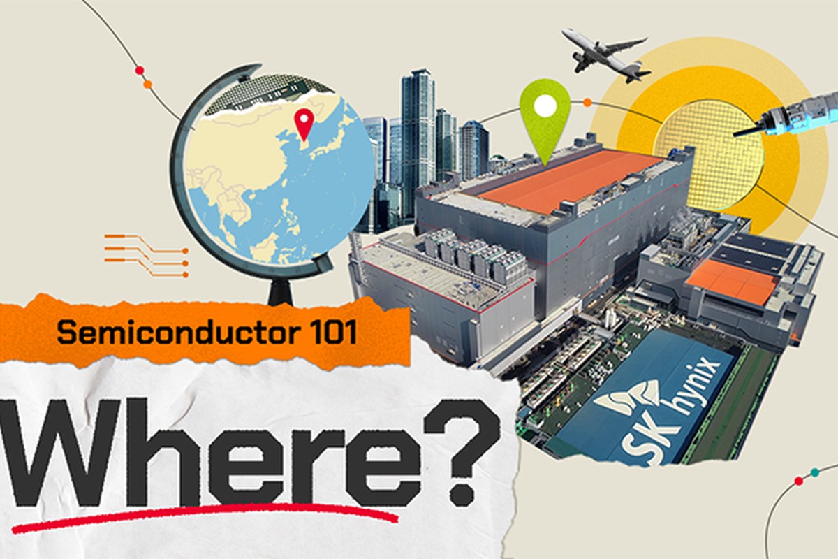
SK Hynix Icheon Campus M10·M14·M16 is a subject of interest in 《Where Semiconductor Manufacturing Takes Place in South Korea》. This operational site acts as a DRAM/R&D hub, where the headquarters and M10·M14·M16 fabs are located. M16, completed in 2021, primarily produces DRAM, while Icheon is introduced as the central hub for R&D and DRAM manufacturing. In this list, the actual function of the SK Hynix Icheon Campus M10·M14·M16 is read from the perspective of 'an industrial map distinguishing operational production bases from AI memory hubs under construction.' Even when compared with similar entries, one should first differentiate the purpose and public status of the SK Hynix Icheon Campus M10·M14·M16.
Recorded confirmation details of SK Hynix Icheon Campus M10·M14·M16 include: Address: 2091 Gyeongchung-daero, Bubal-eup, Icheon-si, Gyeonggi-do · Operational status: Operational DRAM/R&D · Visitor guidelines: Security industrial facility · Unauthorized access and photography prohibited. The coordinates and address of SK Hynix Icheon Campus M10·M14·M16 serve as points of reference to understand industrial locations, not as indications of entrance or potential tour sites. The stages of groundbreaking, completion, equipment installation, operation, and mass production at SK Hynix Icheon Campus M10·M14·M16 are distinct from each other. As a secure enterprise site, unauthorized entry or photography without official guidance is not allowed.
When utilizing SK Hynix Icheon Campus M10·M14·M16 to read industry news, confirm the announcement date, current operational stage, and production or research role in order. By comparing with preceding and succeeding entries, the roles of SK Hynix Icheon Campus M10·M14·M16 within research and development, front-end processing, and back-end processing become clear. The latest official company announcements and local government guidance regarding SK Hynix Icheon Campus M10·M14·M16 take precedence over this description, and directly interpreting investment plans as current production amounts is not an accurate reading method.
Recorded confirmation details of SK Hynix Icheon Campus M10·M14·M16 include: Address: 2091 Gyeongchung-daero, Bubal-eup, Icheon-si, Gyeonggi-do · Operational status: Operational DRAM/R&D · Visitor guidelines: Security industrial facility · Unauthorized access and photography prohibited. The coordinates and address of SK Hynix Icheon Campus M10·M14·M16 serve as points of reference to understand industrial locations, not as indications of entrance or potential tour sites. The stages of groundbreaking, completion, equipment installation, operation, and mass production at SK Hynix Icheon Campus M10·M14·M16 are distinct from each other. As a secure enterprise site, unauthorized entry or photography without official guidance is not allowed.
When utilizing SK Hynix Icheon Campus M10·M14·M16 to read industry news, confirm the announcement date, current operational stage, and production or research role in order. By comparing with preceding and succeeding entries, the roles of SK Hynix Icheon Campus M10·M14·M16 within research and development, front-end processing, and back-end processing become clear. The latest official company announcements and local government guidance regarding SK Hynix Icheon Campus M10·M14·M16 take precedence over this description, and directly interpreting investment plans as current production amounts is not an accurate reading method.
주소 경기도 이천시 부발읍 경충대로 2091
운영 상태 운영·D램/R&D
방문 안내 보안 산업시설·공식 허가 없는 출입 및 촬영 금지
SK hynix Cheongju Campus M15
SK Hynix Cheongju Campus M15
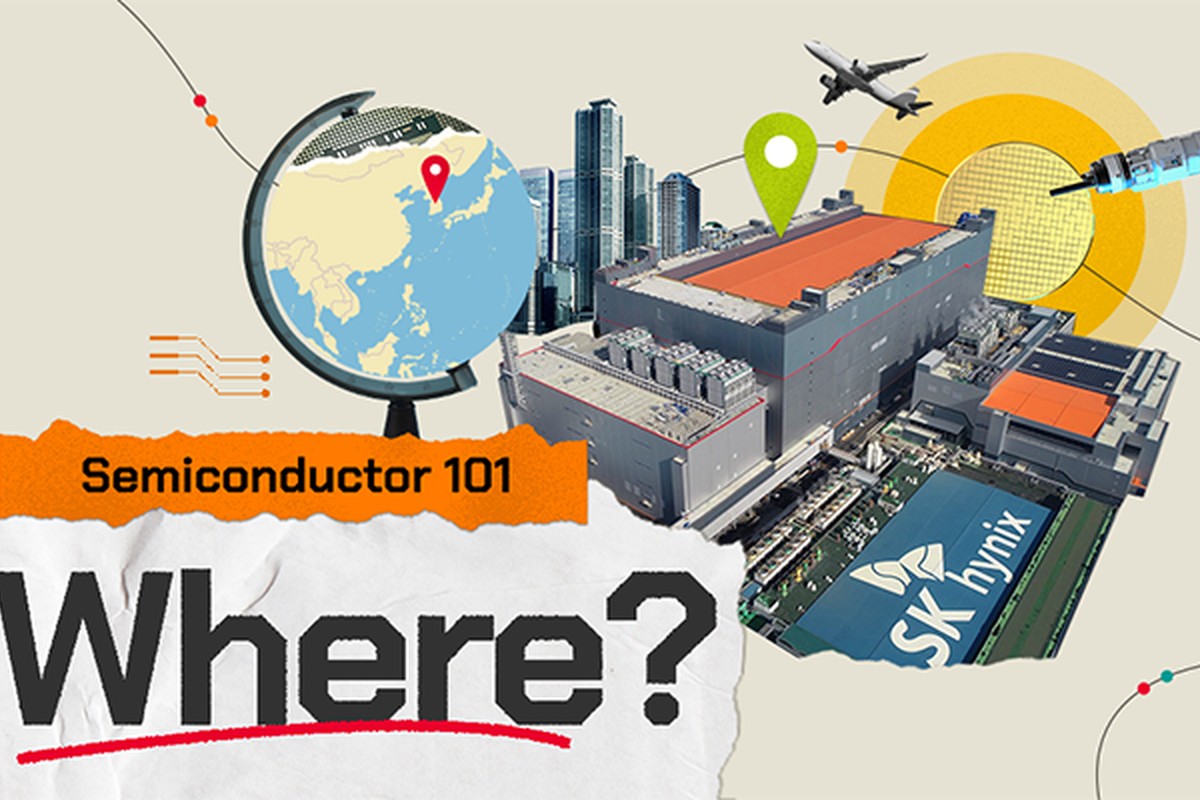
SK Hynix Cheongju Campus M15 is a subject of interest in 《Where Semiconductor Manufacturing Takes Place in South Korea》. This operational site serves as a NAND hub, aiming to strengthen NAND flash production. Differentiating it from the nearby M15X within the Cheongju region reveals the distinctions between existing NAND manufacturing and the next-generation DRAM/HBM expansion. In this list, the actual function of the SK Hynix Cheongju Campus M15 is read from the perspective of 'an industrial map distinguishing operational production bases from AI memory hubs under construction.' Even when compared with similar entries, one should first differentiate the purpose and public status of the SK Hynix Cheongju Campus M15.
Recorded confirmation details of SK Hynix Cheongju Campus M15 include: Address: 215 Daejin-ro, Heungdeok-gu, Cheongju-si, Chungcheongbuk-do · Operational status: Operational NAND · Visitor guidelines: Security industrial facility · Unauthorized access and photography prohibited. The coordinates and address of SK Hynix Cheongju Campus M15 serve as points of reference to understand industrial locations, not as indications of entrance or potential tour sites. The stages of groundbreaking, completion, equipment installation, operation, and mass production at SK Hynix Cheongju Campus M15 are distinct from each other. As a secure enterprise site, unauthorized entry or photography without official guidance is not allowed.
When utilizing SK Hynix Cheongju Campus M15 to read industry news, confirm the announcement date, current operational stage, and production or research role in order. By comparing with preceding and succeeding entries,the roles of SK Hynix Cheongju Campus M15 within research and development, front-end processing, and back-end processing become clear. The latest official company announcements and local government guidance regarding SK Hynix Cheongju Campus M15 take precedence over this description, and directly interpreting investment plans as current production amounts is not an accurate reading method.
Recorded confirmation details of SK Hynix Cheongju Campus M15 include: Address: 215 Daejin-ro, Heungdeok-gu, Cheongju-si, Chungcheongbuk-do · Operational status: Operational NAND · Visitor guidelines: Security industrial facility · Unauthorized access and photography prohibited. The coordinates and address of SK Hynix Cheongju Campus M15 serve as points of reference to understand industrial locations, not as indications of entrance or potential tour sites. The stages of groundbreaking, completion, equipment installation, operation, and mass production at SK Hynix Cheongju Campus M15 are distinct from each other. As a secure enterprise site, unauthorized entry or photography without official guidance is not allowed.
When utilizing SK Hynix Cheongju Campus M15 to read industry news, confirm the announcement date, current operational stage, and production or research role in order. By comparing with preceding and succeeding entries,the roles of SK Hynix Cheongju Campus M15 within research and development, front-end processing, and back-end processing become clear. The latest official company announcements and local government guidance regarding SK Hynix Cheongju Campus M15 take precedence over this description, and directly interpreting investment plans as current production amounts is not an accurate reading method.
주소 충청북도 청주시 흥덕구 대신로 215
운영 상태 운영·낸드
방문 안내 보안 산업시설·공식 허가 없는 출입 및 촬영 금지
SK hynix Cheongju M15X
SK Hynix Cheongju M15X
SK Hynix Cheongju M15X is a subject of interest in 《Where Semiconductor Manufacturing Takes Place in South Korea》. This site is in construction as a next-generation DRAM hub. It is a new fab initiated to expand production capacity for next-generation DRAM, including HBM. The core plan is to connect it with the TSV-based back-end processing capabilities near M15. In this list, the actual function of the SK Hynix Cheongju M15X is read from the perspective of 'an industrial map distinguishing operational production bases from AI memory hubs under construction.' Even when compared with similar entries, one should first differentiate the purpose and public status of the SK Hynix Cheongju M15X.
Recorded confirmation details of SK Hynix Cheongju M15X include: Address: Waeuk-dong, Heungdeok-gu, Cheongju-si, Chungcheongbuk-do · Operational status: Under construction next-generation DRAM · Visitor guidelines: Security industrial facility · Unauthorized access and photography prohibited. The coordinates and address of SK Hynix Cheongju M15X serve as points of reference to understand industrial locations, not as indications of entrance or potential tour sites. The stages of groundbreaking, completion, equipment installation, operation, and mass production at SK Hynix Cheongju M15X are distinct from each other. As a secure enterprise site, unauthorized entry or photography without official guidance is not allowed.
When utilizing SK Hynix Cheongju M15X to read industry news, confirm the announcement date, current operational stage, and production or research role in order. By comparing with preceding and succeeding entries in this list, the roles of SK Hynix Cheongju M15X within research and development, front-end processing, and back-end processing become clear. The latest official company announcements and local government guidance regarding SK Hynix Cheongju M15X take precedence over this description, and directly interpreting investment plans as current production amounts is not an accurate reading method.
Recorded confirmation details of SK Hynix Cheongju M15X include: Address: Waeuk-dong, Heungdeok-gu, Cheongju-si, Chungcheongbuk-do · Operational status: Under construction next-generation DRAM · Visitor guidelines: Security industrial facility · Unauthorized access and photography prohibited. The coordinates and address of SK Hynix Cheongju M15X serve as points of reference to understand industrial locations, not as indications of entrance or potential tour sites. The stages of groundbreaking, completion, equipment installation, operation, and mass production at SK Hynix Cheongju M15X are distinct from each other. As a secure enterprise site, unauthorized entry or photography without official guidance is not allowed.
When utilizing SK Hynix Cheongju M15X to read industry news, confirm the announcement date, current operational stage, and production or research role in order. By comparing with preceding and succeeding entries in this list, the roles of SK Hynix Cheongju M15X within research and development, front-end processing, and back-end processing become clear. The latest official company announcements and local government guidance regarding SK Hynix Cheongju M15X take precedence over this description, and directly interpreting investment plans as current production amounts is not an accurate reading method.
주소 충청북도 청주시 흥덕구 외북동 일원
운영 상태 건설·차세대 D램
방문 안내 보안 산업시설·공식 허가 없는 출입 및 촬영 금지

SK hynix Yongin Semiconductor Cluster
SK Hynix Yongin Semiconductor Cluster
SK Hynix Yongin Semiconductor Cluster is a subject of interest in 《Where Semiconductor Manufacturing Takes Place in South Korea》. This site is currently under construction as a future production base. It is a project where multiple fabs and cooperation complexes are progressively being developed, rather than a completed tourism or production facility. It is planned as a future production hub for AI memory and next-generation DRAM. In this list, the actual function of the SK Hynix Yongin Semiconductor Cluster is read from the perspective of 'an industrial map distinguishing operational production bases from AI memory hubs under construction.' Even when compared with similar entries, one should first differentiate the purpose and public status of the SK Hynix Yongin Semiconductor Cluster.
Recorded confirmation details of SK Hynix Yongin Semiconductor Cluster include: Address: Jukneung-ri, Wonsam-myeon, Cheoin-gu, Yongin-si, Gyeonggi-do · Operational status: Under construction future production base · Visitor guidelines: Security industrial facility · Unauthorized access and photography prohibited. The coordinates and address of SK Hynix Yongin Semiconductor Cluster serve as points of reference to understand industrial locations, not as indications of entrance or potential tour sites. The stages of groundbreaking, completion, equipment installation, operation, and mass production at SK Hynix Yongin Semiconductor Cluster are distinct from each other. As a secure enterprise site, unauthorized entry or photography without official guidance is not allowed.
When utilizing SK Hynix Yongin Semiconductor Cluster to read industry news, confirm the announcement date, current operational stage, and production or research role in order. By comparing with the preceding and succeeding entries, the roles of SK Hynix Yongin Semiconductor Cluster within research and development, front-end processing, and back-end processing become clear. The latest official company announcements and local government guidance regarding SK Hynix Yongin Semiconductor Cluster take precedence over this description, and directly interpreting investment plans as current production amounts is not an accurate reading method.
Recorded confirmation details of SK Hynix Yongin Semiconductor Cluster include: Address: Jukneung-ri, Wonsam-myeon, Cheoin-gu, Yongin-si, Gyeonggi-do · Operational status: Under construction future production base · Visitor guidelines: Security industrial facility · Unauthorized access and photography prohibited. The coordinates and address of SK Hynix Yongin Semiconductor Cluster serve as points of reference to understand industrial locations, not as indications of entrance or potential tour sites. The stages of groundbreaking, completion, equipment installation, operation, and mass production at SK Hynix Yongin Semiconductor Cluster are distinct from each other. As a secure enterprise site, unauthorized entry or photography without official guidance is not allowed.
When utilizing SK Hynix Yongin Semiconductor Cluster to read industry news, confirm the announcement date, current operational stage, and production or research role in order. By comparing with the preceding and succeeding entries, the roles of SK Hynix Yongin Semiconductor Cluster within research and development, front-end processing, and back-end processing become clear. The latest official company announcements and local government guidance regarding SK Hynix Yongin Semiconductor Cluster take precedence over this description, and directly interpreting investment plans as current production amounts is not an accurate reading method.
주소 경기도 용인시 처인구 원삼면 죽능리 일원
운영 상태 건설·미래 생산기지
방문 안내 보안 산업시설·공식 허가 없는 출입 및 촬영 금지
Placing production bases on the map reveals that the phrase 'Korean semiconductor factories' describes a network with distinct functions. Giheung holds the history of research, Hwaseong and Pyeongtaek are at the forefront of advanced processes, Icheon is focused on DRAM and R&D, and Cheongju specializes in NAND and next-generation memory expansions. Yongin should be understood as a site preparing future production capacity, not a completed factory.
When reading related news, prioritize verifying the operational status and product items over the factory names. Terms like 'groundbreaking', 'equipment entrance', and 'mass production' are not interchangeable stages, and announcing investment amounts does not directly mean production has commenced. The map coordinates serve as reference points for understanding industry distribution, not for access guidance. It is safest to check the latest company announcements alongside local transportation and construction information.
When reading related news, prioritize verifying the operational status and product items over the factory names. Terms like 'groundbreaking', 'equipment entrance', and 'mass production' are not interchangeable stages, and announcing investment amounts does not directly mean production has commenced. The map coordinates serve as reference points for understanding industry distribution, not for access guidance. It is safest to check the latest company announcements alongside local transportation and construction information.
At a glance
8 items
Samsung Electronics Giheung Campus
운영·R&D
Samsung Electronics Hwaseong Campus
경기도 화성시 삼성전자로 1운영·생산/R&D
Samsung Electronics Pyeongtaek Campus
경기도 평택시 삼성로 144운영·대규모 생산
Samsung Electronics Onyang Campus
운영·패키지/테스트
SK hynix Icheon Campus M10·M14·M16
운영·D램/R&D
SK hynix Cheongju Campus M15
운영·낸드
SK hynix Cheongju M15X
건설·차세대 D램
SK hynix Yongin Semiconductor Cluster
건설·미래 생산기지
Locations at a glance
8 places
As part of the Coupang Partners program, this post may earn a commission from qualifying purchases.
Comments 0
Log in to leave a comment.
Be the first to comment.
How about these lists?


You might also like


🎲
Not ready to stop here?
Wondering what to read next is the biggest waste of time.
Let the dice decide — you won't know what pops up until you roll.
If you don't press it… won't you wonder forever? 👀